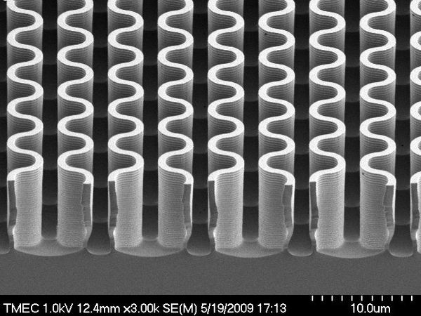
SI MASTER FOR PDMS MOLDING
TMEC offers manufacturing of one to mass Silicon masters (Si mold) for PDMS microfludic channels. Si master allows lower cost for mass manufacturing of PDMS microfluidics compared with the conventional photoresist master thanks to easier cleaning and longer reusability of the Si master compared to coventional photoresist master.
TMEC offers Si master production on 6 inch Silicon wafers (please contact for more details if 8” Si wafer is required). The patterning process for the Silicon master can be done either with a maskaligner (patterning of a whole 6” wafer) or a stepper (multiple dies of max die size of approx. 2cm*2cm on a 6” wafer). TMEC also offers mask making service for the customers' required patterns, please see mask making service in the related section (MASK FABRICATION SERVICES).
The achievable etching uniformity on the channel depth depends on patterning density and pattern design while the through-put will depends on the the etch depth. To find out if we can help you, please send us email wutthinan.jeamsaksiri@nectec.or.th or contact us telling us more about your requirements at 038-857100 ext 136

Post on 2010-11-22 | View 2558

OUR RESEARCH
Oxygen Control on Nanocrystal-AlON Films by Reactive Gas-Timing Technique R.F. Magnetron Sputtering and Annealing Eff
Post on 2009-06-14
The AlON films grown on Si(100) substrates by using radio frequency (r.f.) magnetron sputtering from high purity aluminum (99.999% Al) target with a novel reactive gas-timing techn...